- 您现在的位置:买卖IC网 > Sheet目录409 > DR-TRC103-950-DK (RFM)KIT DEV 950MHZ RFIC SRR
�� �
�
�M� u� lti-b� y� te� C� o� n� fig� u� r� a� tio� n� R� e� g� is� te� r� R� e� a� d�
�n� S� S� _� C� O� N� F� IG�
�S� C� K�
�S� D� I�
�X�
�S� T� A� R� T�
�R� /W�
�A� 4�
�A� 3�
�A� 2�
�A� 1�
�A� 0�
�X�
�S� T� A� R� T�
�R� /W�
�A� 4�
�A� 3�
�A� 2�
�A� 1�
�A� 0�
�X�
�S� T� A� R� T�
�R� /W�
�A� 4�
�A� 3�
�A� 2�
�A� 1�
�A� 0�
�S� T� A� R� T�
�F� ir� s� t� R� e� g� is� te� r� A� d� d� r� e� s� s�
�S� e� c� o� n� d� R� e� g� is� te� r� A� d� d� r� e� s� s�
�T� h� ir� d� R� e� g� is� te� r� A� d� d� r� e� s� s�
�S� D� O�
�H� i-Z�
�X�
�X�
�X�
�X�
�X�
�X�
�X�
�X�
�D� 7�
�D� 6�
�D� 5�
�D� 4�
�D� 3�
�D� 2�
�D� 1�
�D� 0�
�D� 7�
�D� 6�
�D� 5�
�D� 4�
�D� 3�
�D� 2�
�D� 1�
�D� 0�
�F� ir� s� t� R� e� g� is� te� r� V� a� lu� e�
�S� e� c� o� n� d� R� e� g� is� te� r� V� a� lu� e�
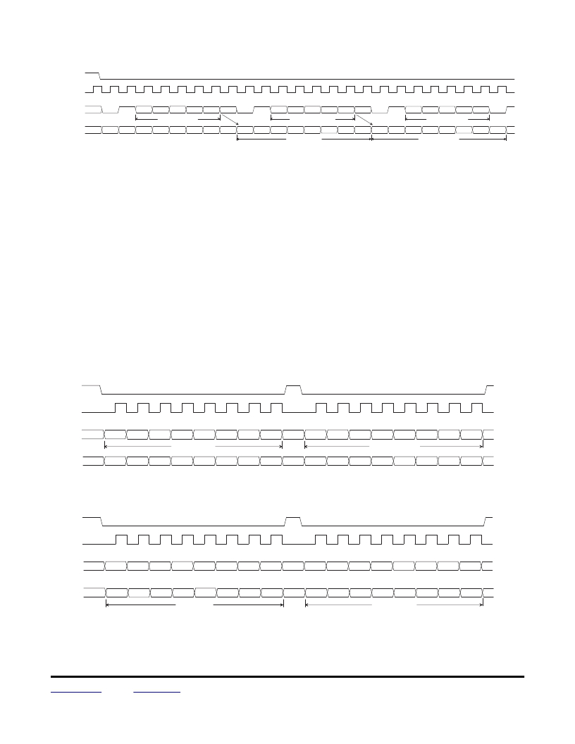
�Figure� 22�
�Multiple� configuration� register� reads� are� also� possible� by� sending� a� series� of� register� addresses� into� the� SPI� port,�
�as� shown� in� Figure� 22.�
�3.11� SPI� Data� FIFO� Interface�
�When� the� transceiver� is� used� in� Buffered� or� Packet� data� mode,� data� is� written� to� and� read� from� the� FIFO� through�
�the� SPI� interface.� Two� interrupts,� IRQ0� and� IRQ1,� are� used� to� manage� the� transfer� procedure.�
�When� the� transceiver� is� operating� in� Buffered� or� Packet� data� mode,� the� FIFO� interface� is� selected� when�
�nSS_DATA� is� set� to� 0� and� nSS_CONFIG� is� set� to� 1.� SPI� operations� with� the� FIFO� are� similar� to� operations� with�
�the� configuration� registers� with� two� important� exceptions.� First,� no� addresses� are� used� with� the� FIFO,� only� data�
�bytes� are� exchanged.� Second,� nSS_DATA� must� be� toggled� high� and� back� low� between� data� bytes� when� writing�
�to� the� FIFO� or� reading� from� the� FIFO.� Toggling� nSS_DATA� indexes� the� access� pointer� to� each� byte� in� the� FIFO� in�
�lieu� of� using� explicit� addressing.� Figure� 23� shows� the� timing� diagram� for� a� multiple-byte� write� sequence� to� the�
�TRC103� during� transmit,� and� Figure� 24� shows� the� timing� for� a� multi-byte� read� sequence.�
�T� R� C� 1� 0� 3� D� a� ta� W� r� ite� to� F� IF� O�
�n� S� S� _� D� A� T� A�
�S� C� K�
�S� D� I�
�X�
�D� 7�
�D� 6�
�D� 5�
�D� 4�
�D� 3�
�D� 2�
�D� 1�
�D� 0�
�X�
�D� 7�
�D� 6�
�D� 5�
�D� 4�
�D� 3�
�D� 2�
�D� 1�
�D� 0�
�F� ir� s� t� B� y� te� W� r� itte� n�
�S� e� c� o� n� d� B� y� te� W� r� itte� n�
�S� D� O�
�H� i-Z�
�X�
�X�
�X�
�X�
�X�
�X�
�X�
�X�
�H� i-Z�
�X�
�X�
�X�
�X�
�X�
�X�
�X�
�X�
�H i-Z�
�Figure� 23�
�n� S� S� _� D� A� T� A�
�S� C� K�
�T� R� C� 1� 0� 3� D� a� ta� R� e� a� d� fro� m�
�F� IF� O�
�S� D� I�
�X�
�X�
�X�
�X�
�X�
�X�
�X�
�X�
�X�
�X�
�X�
�X�
�X�
�X�
�X�
�X�
�X�
�X�
�S� D� O�
�H� i-Z�
�D� 7�
�D� 6�
�D� 5�
�D� 4�
�D� 3�
�D� 2�
�D� 1�
�D� 0�
�H� i-Z�
�D� 7�
�D� 6�
�D� 5�
�D� 4�
�D� 3�
�D� 2�
�D� 1�
�D� 0�
�H� i-Z�
�F� ir� s� t� B� y� te� R� e� a� d�
�Figure� 24�
�S� e� c� o� n� d� B� y� te� R� e� a� d�
�www.RFM.com� E-mail:� info@rfm.com�
�?� 2009-2010� by� RF� Monolithics,� Inc.�
�Technical� support� +1.800.704.6079�
�Page� 27� of� 65�
�TRC103� -� 11/29/12�
�发布紧急采购,3分钟左右您将得到回复。
相关PDF资料
DR-TRC105-372-DK
DEV KIT TRC105
DR-TRC105-450-EV
BOARD EVALUATION 450MHZ RFM RFIC
DR-TXC100-433
BOARD EVALUATION 433MHZ TXC100
DR-WLS1273L-EV
KIT EVAL FOR WLS1273L
DR7000-DK
3G DEVELOPMENT KIT 433.92MHZ
DR7001-DK
3G DEVELOPMENT KIT 315 MHZ
DR7003-DK
3G DEVELOPMENT KIT 303.825 MHZ
DR8000-DK
3G DEVELOPMENT KIT 916MHZ
相关代理商/技术参数
DR-TRC103-950-EV
功能描述:BOARD EVALUATION 950MHZ RFM RFIC RoHS:否 类别:RF/IF 和 RFID >> RF 评估和开发套件,板 系列:- 标准包装:1 系列:- 类型:GPS 接收器 频率:1575MHz 适用于相关产品:- 已供物品:模块 其它名称:SER3796
DR-TRC104-2400-DK
功能描述:射频开发工具 TRC104 Development Kit 2.4 GHz RoHS:否 制造商:Taiyo Yuden 产品:Wireless Modules 类型:Wireless Audio 工具用于评估:WYSAAVDX7 频率: 工作电源电压:3.4 V to 5.5 V
DR-TRC104-2400-EV
制造商:RFM 功能描述:BOARD EVALUATION 2.4GHZ RFM RFIC
DR-TRC105-304-DK
功能描述:射频开发工具 TRC105 Development Kit 303-307 MHz RoHS:否 制造商:Taiyo Yuden 产品:Wireless Modules 类型:Wireless Audio 工具用于评估:WYSAAVDX7 频率: 工作电源电压:3.4 V to 5.5 V
DR-TRC105-304-EV
功能描述:射频开发工具 TRC105 Evaluation Board 303-307 MHz RoHS:否 制造商:Taiyo Yuden 产品:Wireless Modules 类型:Wireless Audio 工具用于评估:WYSAAVDX7 频率: 工作电源电压:3.4 V to 5.5 V
DR-TRC105-315-DK
功能描述:射频开发工具 TRC105 Development Kit 310-319 MHz RoHS:否 制造商:Taiyo Yuden 产品:Wireless Modules 类型:Wireless Audio 工具用于评估:WYSAAVDX7 频率: 工作电源电压:3.4 V to 5.5 V
DR-TRC105-315-EV
功能描述:射频开发工具 TRC105 Evaluation Board 310-319 MHz RoHS:否 制造商:Taiyo Yuden 产品:Wireless Modules 类型:Wireless Audio 工具用于评估:WYSAAVDX7 频率: 工作电源电压:3.4 V to 5.5 V
DR-TRC105-345-DK
功能描述:射频开发工具 TRC105 Development Kit 342-348 MHz RoHS:否 制造商:Taiyo Yuden 产品:Wireless Modules 类型:Wireless Audio 工具用于评估:WYSAAVDX7 频率: 工作电源电压:3.4 V to 5.5 V